The Imaging endstation (EH1) is made up of many parts. Here we list the pieces of hardware and those specs that are important for planning your experiments.
Sample stages
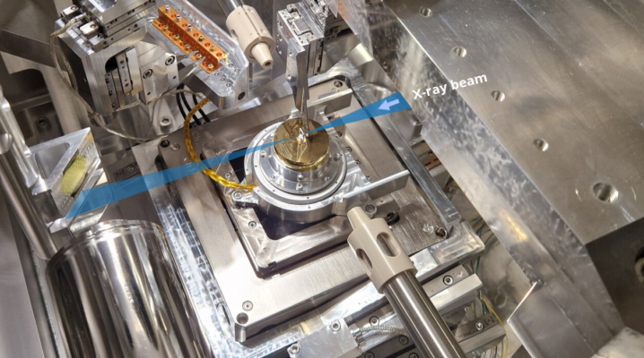
For fine scanning of the sample through the X-ray beam an in-vacuum scanner stage from nPoint is used. The scanning stage has the following specifications of interest for the user:
| Closed-loop Travel | 200 µm | 200 µm | 100 µm (vertical) |
| Position Noise | 0.7nm | 0.7nm | 0.3nm |
| Resonant Frequency | 350Hz | 350Hz | 450Hz |
| Linearity Deviation | 0.01% | 0.01% | 0.02% |
A rotation stage SR-5714C (from SmarAct, Germany) is mounted on top of the scanner to rotate the sample either for tomographic measurements or to align it to the X-ray beam at an specific angle. The stage is mounted such that the axis of rotation is in a vertical orientation.
| angular travel | ∞ [°] |
| closed loop-Loop angular resolution | < 15 [0.001 * °] |
| sphere of confusion | < 1 µm radially < 0.5 µm along the rotation axis |
Detectors
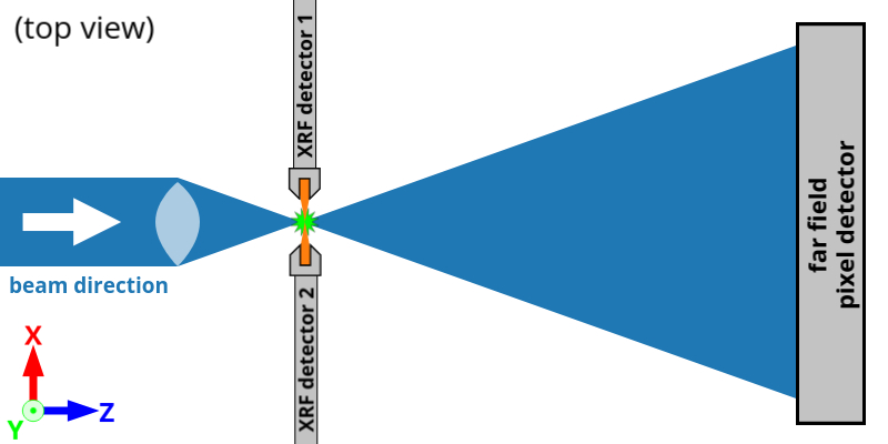
The Imaging endstation (EH1) has two types of detectors for X-rays: a 2D pixel detector for X-ray ptychoghraphy measurements and two energy dispersive silicon drift detectors for X-ray fluorescence measurements. All detector sensors are located inside the vacuum chamber. The arrangement of the detectors relative to the probing beam, the focus and to each other is shown in the sketch above.
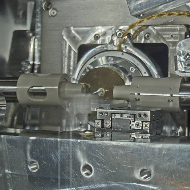
For X-ray fluorescence measurements we have two single-element silicon drift detectors “SDD” (from RaySpec, United Kingdom) with carbon entry windows connected to a pulse processor Xspress3-Mini (from Quantum Detectors, United Kingdom). The key specs of the detectors are:
| sensor material | Si |
| sensor area | collimated to 50 mm² |
| sensor thickness | 450 µm |
| window material | 1 µm thick graphene |
| energy resolution | ≤133 eV FWHM (at 5.9 keV) |
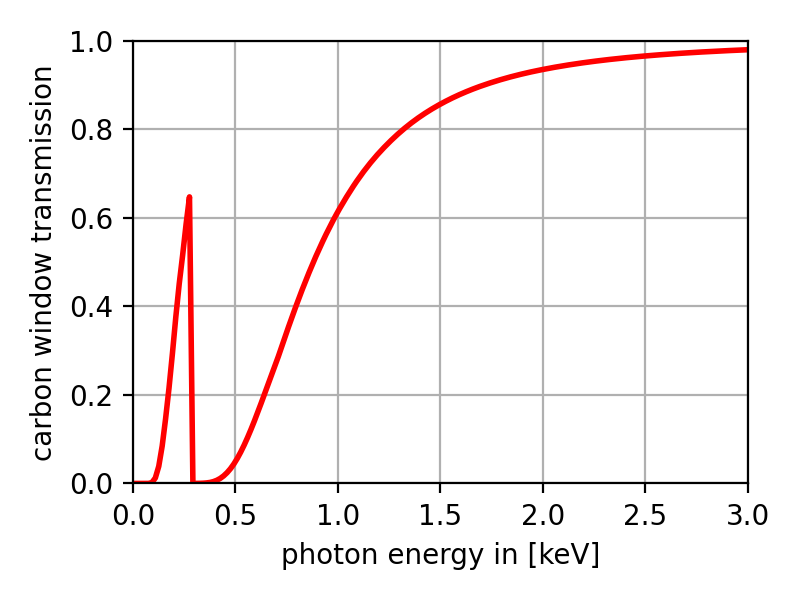
The active detector area is protected by a 1 µm thick window made from carbon. In the graph above the photon energy dependent transmission of this window is plotted. The low transmission at the lower photon energies and the increased electronic noise of the readout electronics limit meaningful XRF measurements to chemical elements with an atomic number of 11 (sodium) or higher.
The Xspress3-Mini pulse processor has a deadtime of about ~80 ns per event and allows to process about one million XRF photons per second.
Collimators manufactured from PEEK are mounted at the end of both detector heads. These reduce the background signal from stray photons from other places than the sample (for example from secondary XRF photons). Both detectors are motorized to the be moved closer to / further from the sample. The closest distance of the active detector area to the X-ray beam is 30 mm.
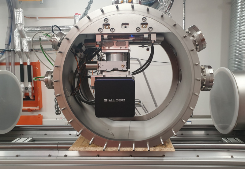
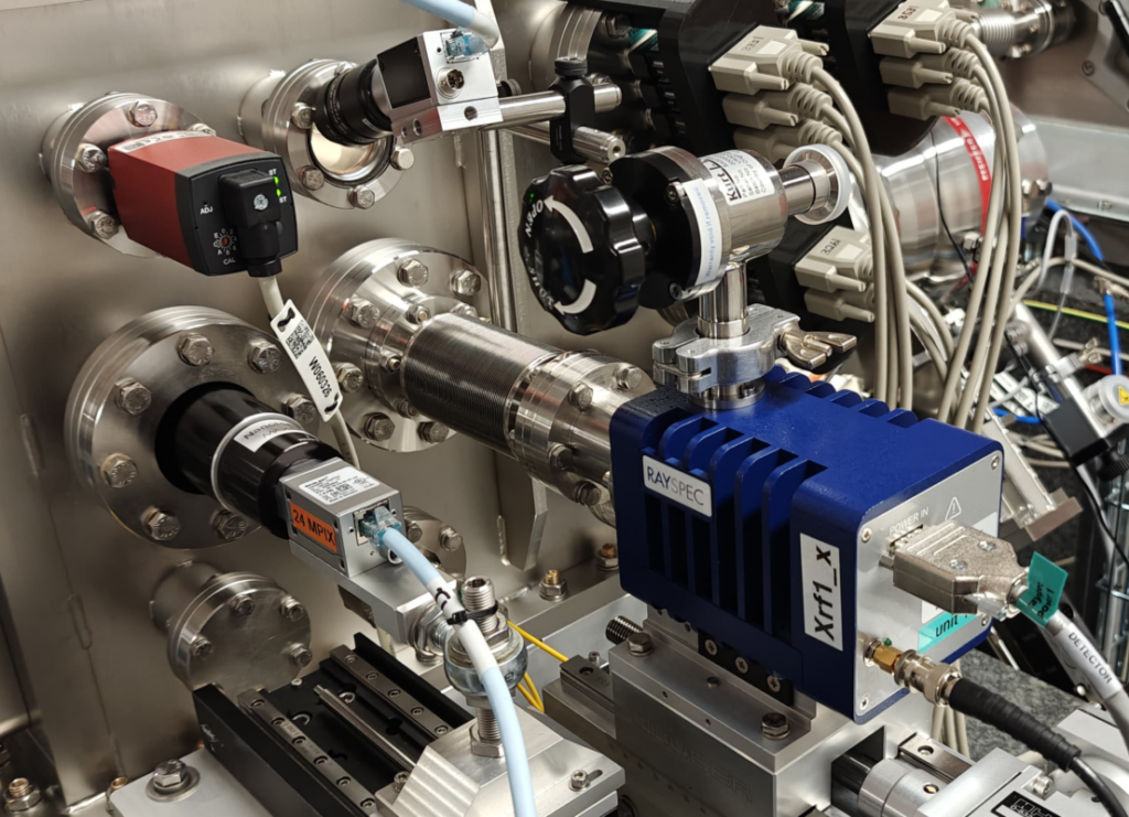
For ptychographic measurements we have a photon counting pixel detector EIGER2 X 4M (from DECTRIS, Switzerland). The detector is mounted fully in vacuum without any window. The following detector specs might be of interest:
| pixel size | 75 μm x 75 μm |
| number of pixels (h x v) | 2068 x 2162 = 4 471 016 |
| active area (h x v) | 155.2 mm x 162.5 mm |
| sensor material | Si |
| sensor thickness | 450 μm |
| energy range | 6 keV – 40 keV |
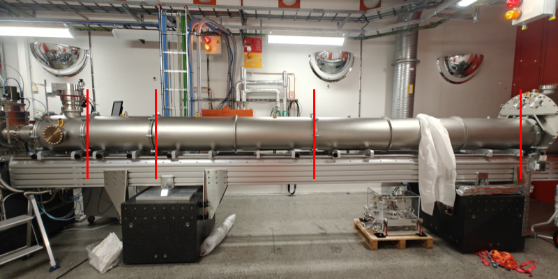
In the most common configuration it is placed at a distance of 7.1m from the X-ray focus / sample position. This is the furthest sample detector position. This distance is not motorized, but can still be adjusted. The flight tube is made of segments of various lengths. By shuffling around segments a few discrete distances can be achieved. As changing the distance requires venting, rearrangement of the segments and finally pumping the flight tube again, this is not something we would do during a beamtime.