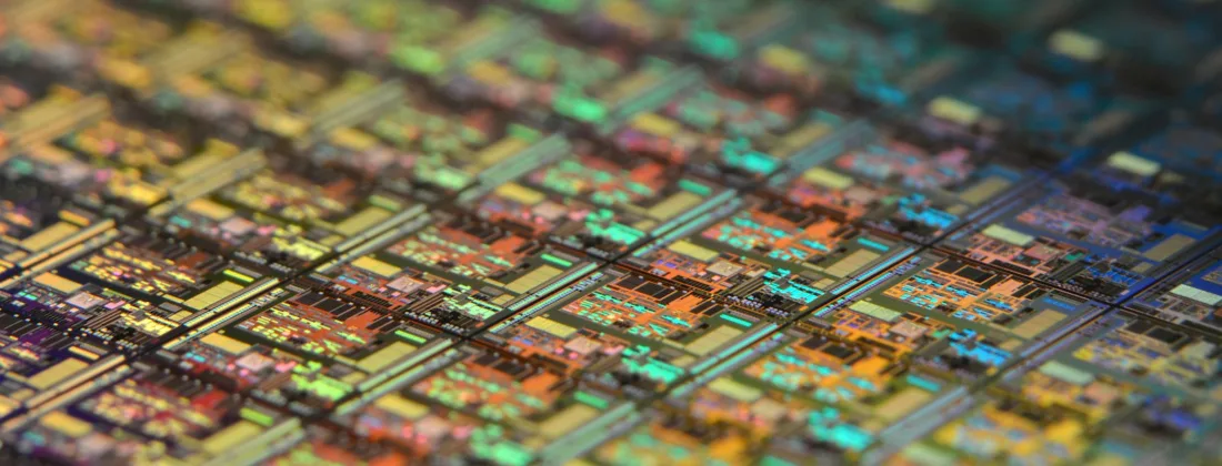
A modern chip contains billions of transistors. The size of individual features is just a couple of tens of nanometres. With decreasing size follows increased demands on material control and characterisation down to the atomic scale. The nano-focused X-ray beam at beamline NanoMAX prove to be a useful tool for investigating electromigration, a significant cause of failure in on-chip interconnects.
Electromigration and failure
Copper is the most commonly used material for connecting transistors on a chip. The current being pushed through the tiny copper wires cause a phenomenon called electromigration. Electromigration is a form of mass transport driven by the flow of electrons, where atoms migrate from one end of the copper structure to the other, changing the structure and leading to short circuits or disconnects. When the wire gets smaller it means that a higher current will be pushed through and the resulting electromigration can cause failure in the circuit.
“Electromigration is one of the biggest reliability issues in integrated circuits and although it has been widely studied the interplay between the different forces that drive or counteract electromigration is not completely understood,” says Professor Sten Vollebregt from Delft University of Technology.
Nano focus reveals structural details
Copper structures of different lengths and thicknesses were fabricated on top of a substrate, a piece of silicon prepared with layers of silicon dioxide and titanium nitride, to simulate the situation on the chip. The structures were heated and had current run through them to induce electromigration.
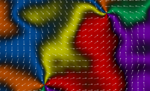
After the preparation, the samples were investigated at the NanoMAX beamline using a beam focused into a 62 nanometre diameter spot. The experiment gives information about the distance between the atoms in the copper, which in turn reveals stresses in the material.
“We found two different stages, where the stress is initially controlled by the difference in thermal expansion between the silicon substrate and the copper line structure, but later the stresses developing during electromigration become dominant. A better understanding of the stress within the interconnect during electromigration will allow the development of improved models, resulting in better prediction of the reliability. This will ultimately help manufacturers design more reliable and perhaps even smaller chips,” says Magnus Colliander from Chalmers University of Technology.
Towards studies during electromigration
In the present study, the stresses are measured after the fact. The next step is to perform the study in situ, that is, at the same as heating and running current through the copper structures and inducing electromigration.
“In the future, we plan to explore more different metals and conditions. Due to the extremely small scale of interconnects and the complex metal stacks studying actual working chips is difficult. Instead, we are measuring on model chips. Using these results for development and calibration will allow us to understand the behaviour of real chips under complex operation conditions”, concludes Sten Vollebregt.
Photo: Laura Ockel/Unsplash